The Ham that utilize an Analogic Satellite Receivers to receive the
1,2GHz ATV band well knows that without the adoption of a Low Noise
Preamplifier the results frequently are scarce and deludent so to
discourage the novices.
A similar situation is valid also for the RF Modules commons into the Ham
markets at a low price. The fundamental problem is that the front-end
stages used in these circuits rarely have a Noise Figure less than 8dB!
In a typical using of a Sat-RX is the Down-Converter to provide for this
primarily necessity with a typical NF much less than 1dB.
The follow project realize a Very Low Noise Preamplifier by the using of
an HEMT (High Electron Mobility Transistor) into the first stage where the
gain at 1.25GHz already is 19dB with a Nf<=0.4dB. The circuit also adopts
two important filters that offer a shooting down of 50dB on the strong
Cellular's signals present in the nearest 900MHz spectrum.
The final result obtained really is excellent !
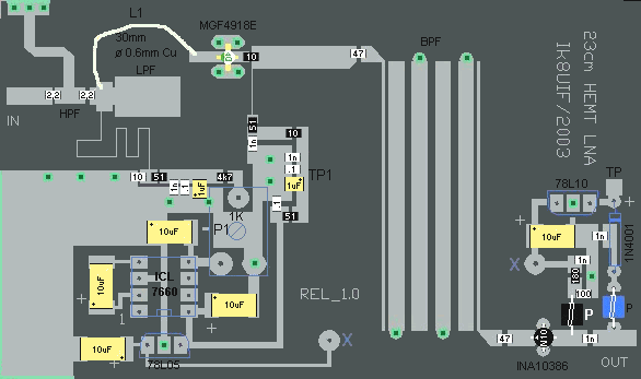
CIRCUIT DIAGRAM
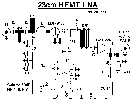 On the RF input is placed a first High Pass Filter (HPF) then follow a Low
Pass Filter (LPF) to cut all frequency > 1,7GHz.
The inductor L, besides adapt the input impedance of the first stage,
allows the tuning for the minimum Noise Figure.
The HEMT adopted is an MGF4918E, common into surplus markets. It offers a
Gain =>19dB at 1250MHz with a NF<=0.4dB.
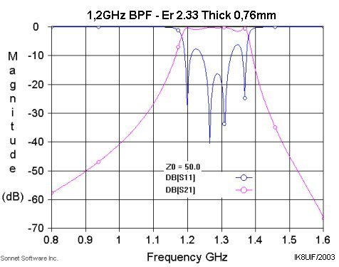
After the first amp stage follows a 4 pole interdigited Band Pass Filter
(BPF) that carries out a clean band preselection on 1,25GHz.
For the optimization of this filter I've used the Sonnet© simulations
software release 8.51.
Here the graph of Magnitude/Frequency obtained on BPF:
On the RF input is placed a first High Pass Filter (HPF) then follow a Low
Pass Filter (LPF) to cut all frequency > 1,7GHz.
The inductor L, besides adapt the input impedance of the first stage,
allows the tuning for the minimum Noise Figure.
The HEMT adopted is an MGF4918E, common into surplus markets. It offers a
Gain =>19dB at 1250MHz with a NF<=0.4dB.
After the first amp stage follows a 4 pole interdigited Band Pass Filter
(BPF) that carries out a clean band preselection on 1,25GHz.
For the optimization of this filter I've used the Sonnet© simulations
software release 8.51.
Here the graph of Magnitude/Frequency obtained on BPF:
 The MMIC INA10386 adding a 20dB gain but it's possible to omit it (like
into my prototype) since the gain of the Hemt is oneself sufficient in
many applications.
The BIAS voltage for the HEMT is generated by the classic 7660 i.c. and
it's regulated by the trimmer P1.
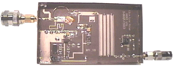
PCB & COMPONENTS LAYOUT
The MMIC INA10386 adding a 20dB gain but it's possible to omit it (like
into my prototype) since the gain of the Hemt is oneself sufficient in
many applications.
The BIAS voltage for the HEMT is generated by the classic 7660 i.c. and
it's regulated by the trimmer P1.
PCB & COMPONENTS LAYOUT 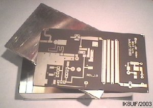
The PCB is realized on a Teflon
board with an Er=2.33 and a
Thickness=0.76mm. The RT5870 or
DI-CLAD 870 or MY3-30 works well.
Pcb's layout (PDF) is available in
Download:
IK8UIF - PRE12R10.PDF
To obtain correct PCB dimension
un-check all regulations into
Acrobat Reader Print menu.
Components' layout:
 The GREEN pads are connected to the GND pcb side by the utilize of a
series of tinned PINS with a diameter of 0.8mm.
Wiring the X pads on the gnd side of pcb. On the GND side are placed all
the components drawed with the CYANO color: 78L10, 78L05, Ferrite Pearlins,
1N4001, 7660 and the 1k trimmer. The P inductors are realized winding
2 turns of 0.3mm copper wire on a 3mm Ferrite Pearl.
The inductor L is 30mm long and realized with a 0.6mm silver-copper wire.
This inductor initially is mounted FLAT on the pcb and this distance will
be tuned to obtain the minimum Noise Figure.
Tune the P1 trimmer to obtain a reading of 3.8-4 volts on TP1 (use an high
impedance voltmeter).
If the INA10386 is omitted remember to short his in/out pads with a 0.8mm
silver-copper wire.
TUNING
The tuning of the preamplifier consists to obtain the lowest Noise Figure.
The GREEN pads are connected to the GND pcb side by the utilize of a
series of tinned PINS with a diameter of 0.8mm.
Wiring the X pads on the gnd side of pcb. On the GND side are placed all
the components drawed with the CYANO color: 78L10, 78L05, Ferrite Pearlins,
1N4001, 7660 and the 1k trimmer. The P inductors are realized winding
2 turns of 0.3mm copper wire on a 3mm Ferrite Pearl.
The inductor L is 30mm long and realized with a 0.6mm silver-copper wire.
This inductor initially is mounted FLAT on the pcb and this distance will
be tuned to obtain the minimum Noise Figure.
Tune the P1 trimmer to obtain a reading of 3.8-4 volts on TP1 (use an high
impedance voltmeter).
If the INA10386 is omitted remember to short his in/out pads with a 0.8mm
silver-copper wire.
TUNING
The tuning of the preamplifier consists to obtain the lowest Noise Figure.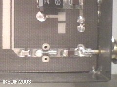 For this scope is required an adequate
instrumentations' laboratory with a Panfi
to act the measuring of the very low NF.
In any case it's possible to obtain NF=0.4dB
with the inductor L mounted as much flat on
the pcb and tuning the trimmer P1 for abt 4
volts on the test point TP1.
I advise to mount the INA10386 after
testing the preamplifier only with the hemt
MGF4918. Maybe you'll keep this final
solutions...
Follows the measures of Band Width and Gain of the prototype with only the
MGF4918 mounted:
For this scope is required an adequate
instrumentations' laboratory with a Panfi
to act the measuring of the very low NF.
In any case it's possible to obtain NF=0.4dB
with the inductor L mounted as much flat on
the pcb and tuning the trimmer P1 for abt 4
volts on the test point TP1.
I advise to mount the INA10386 after
testing the preamplifier only with the hemt
MGF4918. Maybe you'll keep this final
solutions...
Follows the measures of Band Width and Gain of the prototype with only the
MGF4918 mounted:
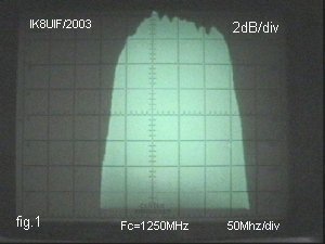
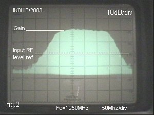
Test Setup
- Sweep Generator HP8620A + 86222A (0.01÷2.4GHz)
- Spectrum Analyzer HP141T + 8555A + 8552B
- 80dB (5x16) SMA Attenuator
Good realization !
73s de Ik8UIF Alberto